
How to Elevate RRAM and MRAM Design Experience to the Next Level
Embedded non-volatile memory (eNVM) is a vital element in modern electronic devices as a storage solution that retains data even when power is turned off. Aside from existing non-volatile memory technology like One-Time-Programmable memory (OTP), Multiple-Time-Programmable memory (MTP) and Flash memory (Flash), emerging non-volatile memories such as Resistive Random Access Memory (RRAM) and Magneto-resistive Random Access Memory (MRAM) have received significant attention. Both are considered next-generation technologies that could revolutionize electronic memory. This article will explore the potential advantages of RRAM and MRAM in various applications and elucidate why such new technologies are imperative to address future memory demands, as well as some challenges designers may encounter in the implementation.
Exploring the Benefits of Emerging Memory
Why do RRAM and MRAM capture the attention of the industry? The answer lies in scalability. RRAM relies on the change in resistance within a dielectric material to store data, featuring low-voltage operation and low-power consumption. MRAM, on the other hand, uses the orientation of magnetic fields to store data and boasts high-speed operation and non-volatility. Figure 1 illustrates the positioning of different types of NVM. As the semiconductor process goes below 28nm, existing non-volatile memory utilizing floating-gate technology no longer scales effectively. It becomes more difficult to retain the data in floating-gates and thus requires more process steps and more masks to construct a robust memory cell structure. Therefore, emerging technologies like RRAM and MRAM have become more appealing to chip designers as they are much easier to be integrated into advance node processes. With RRAM and MRAM, only two or three additional masks are needed in the back end of a standard CMOS process.
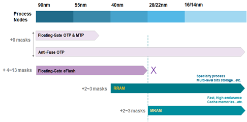
Figure 1. Positioning of RRAM and MRAM
Reduced process steps and fewer masks play a crucial role in cutting down manufacturing costs and time, particularly important for specialty processes like HV and BCD processes, known for their complexity compared to the standard CMOS platform. This streamlined approach enhances the flexibility of RRAM and MRAM in a wide range of applications beyond advanced logic controllers. Currently, research and development are underway to integrate RRAM into analog/mix-mode ICs like PMICs or display driver ICs.
Furthermore, both RRAM and MRAM offer notable advantages. The multi-level bits storage of RRAM allows for high-density neural networks and computing-in-memory architectures, while the non-volatility and fast read-write capabilities of MRAM make it ideal for non-volatile caches in applications like SSD controllers and FPGAs, enabling instant-on functionality and preventing data loss during power interruptions.
Navigating the Challenges Ahead
While RRAM and MRAM beat out embedded Flash in many ways, adopting these emerging technologies also poses challenges in terms of integration and design. The analog/mixed-signal nature of RRAM and MRAM requires expertise in precise circuit design for read/write operations. For example, MRAM is sensitive to read disturbs and requires a fast speed. This necessitates careful sense amplifier design, making the overall design process more difficult and complex. For RRAM, since a forming step to establish the conductive filament in the cell is needed, it often requires pre-cycling to stabilize its behavior. Accurate control of voltages and timing during set/reset operations is also critical for ensuring its reliability.
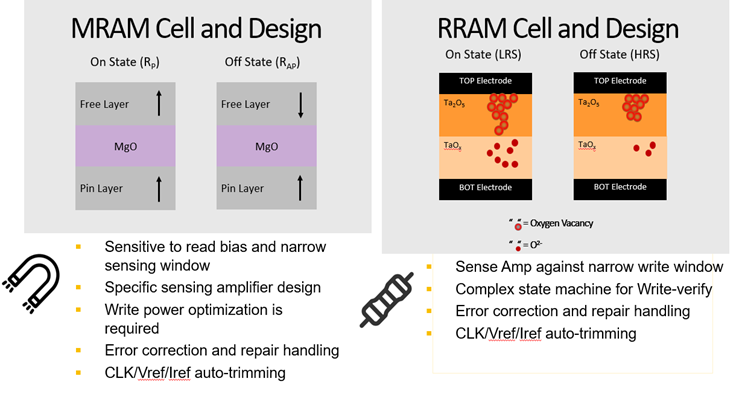
Figure 2 Design challenges of embedded RRAM and MRAM
Additionally, both RRAM and MRAM need redundancy and error-correcting codes (ECC) to enhance yields, inevitably leading to increasing costs in size. Therefore, the trade-off between yields and area footprint becomes an important consideration in the design of embedded RRAM and MRAM IPs. Successful designs for RRAM/MRAM require comprehensive manufacturing knowledge as well. DFT, BIST, BISR, and JTAG interface mechanisms are crucial in determining testing time and cost. Optimal design therefore relies on the expertise of dedicated IP professionals.
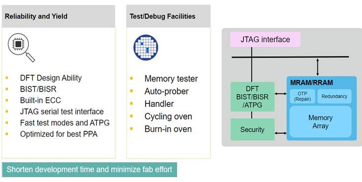
Figure 3 Design services of embedded RRAM and MRAM
Enabling Seamless Design with eMemory
As the increasing design complexity introduced by emerging memory technologies, partnering with an experienced eNVM IP provider becomes even more pronounced. eMemory, as a world-leading eNVM provider, has delivered best-in-class designs to top foundries and fabless companies. Specialized in CMOS-compatible OTP and MTP solutions, eMemory also provides the RRAM and MRAM design services to help customers with cutting-edge embedded memory IPs. eMemory’s RRAM solution is now available on UMC 40nm ULP and 22nm ULL platforms, with the design kit ready for implementation. Our future RRAM roadmap will progress toward lower I/O voltages and higher operating temperature for automotive-grade applications. At the same time, eMemory is committed to MRAM development with major foundries and MRAM companies; characterization of one of our MRAM projects on a 22nm platform has been completed and is currently undergoing qualification.
Professional design services not only accelerate the design process but also save valuable product development resources. For IC design houses seeking novel eNVM solutions, minimizing time-to-market is of paramount importance. eMemory’s RRAM development on a new foundry platform can be completed in just 1.5 to 2 years, depending on the manufacturing schedules. Customization of the RRAM IP on a qualified process platform can be achieved within one year or even less.
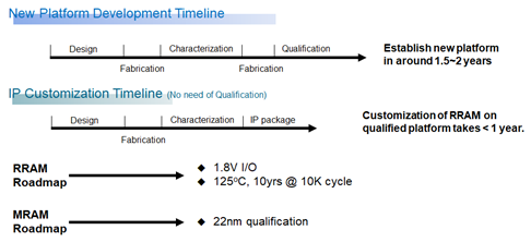
Figure 4 Development timeline and roadmap
As the largest pure eNVM IP provider in the world with the widest OTP/MTP IP availability across major foundries, eMemory has unmatched track records of eNVM IP production. We work closely with foundries, FA (Failure Analysis) and packaging houses to deliver verified, reusable, and reliable memory to our customers. Furthermore, eMemory and its subsidiary, PUFsecurity, have complete hardware security solutions, consisting of OTP and PUF, to safeguard the data stored in RRAM and MRAM. The OTP is an indispensable IP block for analog trimming, memory array hard-repair and encryption key storage; its combination with PUF-based IP can further provide a true hardware root of trust (HRoT) solution. As substitutes for eFlash in advanced nodes, MRAM and RRAM are expected to incorporate security mechanisms same as existing flash memories to protect the data and programs stored in the memory.
Partnering with a leading eNVM IP provider not only reduces the risk but also ensures effective emerging memory integration. With expertise across various embedded memory solutions, from mature programmable memories to cutting-edge RRAM and MRAM, eMemory offers comprehensive technical support, empowering designers to reduce integration risks and expedite time-to-market. As manufacturing processes and IP solutions of RRAM and MRAM continue to advance, their unique characteristics create opportunities for innovation across diverse applications from IoT to automotive and beyond.
To know more about eMemory’s RRAM and MRAM solutions, click here.