Tackling the Challenges of Advanced Silicon Chips: an Innovative Approach to Safe and Reliable SRAM Repair
The Rising Demand for Higher SRAM Density in AI and DPU Applications
Along with the rise of the Internet of Things (IoT), mobile devices, and edge computing, the boom of AI-enhanced features has enabled applications to add in even greater functionality, such as intelligent sensing, in-vehicle driver assistance (ADAS), voice recognition, etc., all of which require the use of increasingly larger training models. However, as the progress of CPU performance slows, new ideas to reduce the IO and data loading on CPUs are becoming more popular. These include such solutions as DPU or PIM (Process in Memory) architectures, as well as the introduction of hierarchical data processing. However, as more CPUs are required for hierarchical processing, there is a corresponding need for more SRAM caches to serve these high-speed CPUs. Thus, the increasing popularity of AI applications and DPU architecture implementations has led to the growing demand for higher SRAM densities.
Challenges to SRAM Yield and Reliability with the Development of Advanced Processes
SRAM is a major driving force behind the advancement of CMOS technology, and with the rise of AI applications, the amount of on-chip SRAM is expected to soar from tens to hundreds of MB. In principle, the higher the density of the SRAM, the higher the chances of producing bad cells, a non-trivial threat to wafer yields. In addition, there are other challenges to solve during the development of a new process technology:
One is that photolithography and etching technologies are no longer able to advance in accordance with Moore's Law as previously seen, even for the latest FinFET technologies. As a result, transistor sizes and metal pitches cannot be reduced as much, so that each successive generation of SRAM memory cells may not be shrunk as much as before.
The second is that as feature sizes shrink and transistor density increases, the power consumed by the transistors leads to an even higher rise in die temperature. This in turn causes the static leakage current of the transistors to rise, resulting in a decrease in the SRAM Static Noise Margin (SNM).
Due to the above challenges to SRAM yield and reliability, the ability to repair SRAMs has become very important.
Understand the Mechanisms Behind Memory Repair
Memory repair technology adds redundant rows or columns to the memory array so that defective primary memory cells can be replaced with spare ones as needed. As a result, even if part of the embedded memory array is defective after manufacturing, it can be repaired and prevent the waste of binning the entire chip.
Originally, the process of testing, analyzing and repairing memory was performed manually, requiring the use of additional, specialized test equipment. However, as designs became more complex and testing took longer, improvements were sought to speed up the testing process, with one such innovation being the development of built-in self-test (BIST) and repair (BISR) units. Memory BISR (MBISR) makes diagnostics and repair much easier for the tester than using a manual process. Automatically importing tests and performing repair not only saves time, money and equipment resources, but also eliminates the bandwidth limitations of external memory testers.
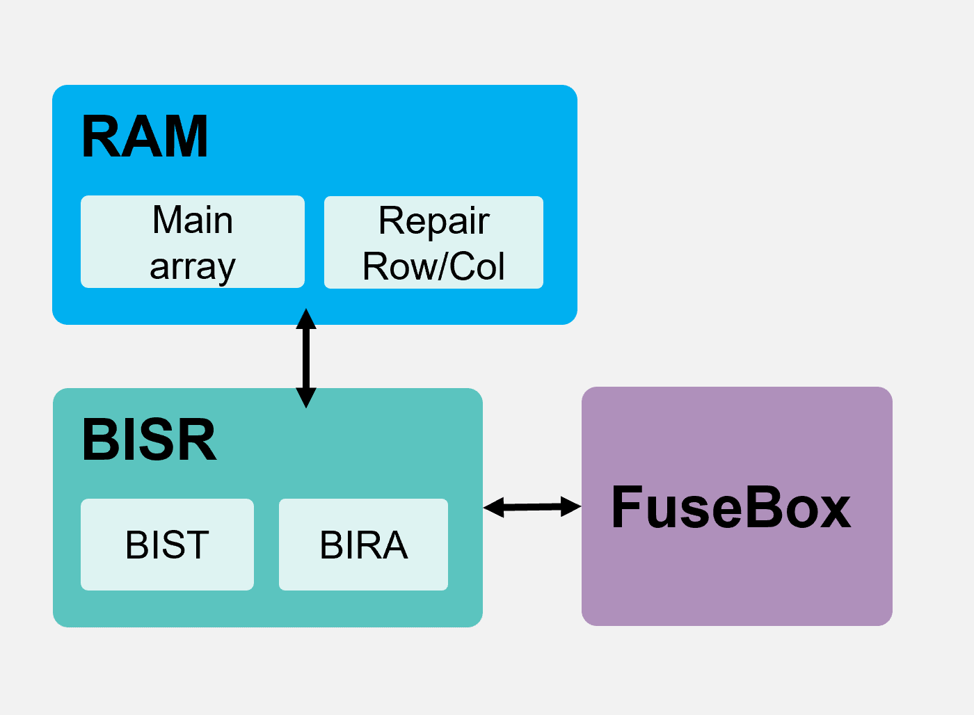
A typical MBISR setup consists of built-in testing (MBIST), remediation analysis (MBIRA), and a FuseBox module, with the BIST module testing the primary and redundant storage units to identify those that are good or are defective. The MBIRA module can then assign the good redundant units to replace the defective primary memory units. After this repair analysis is complete, a permanent record of the memory array "repair signature" is written to a dedicated memory (commonly known as a FuseBox).

Figure 1: MBISR Setup
Why is OTP a Better Choice?
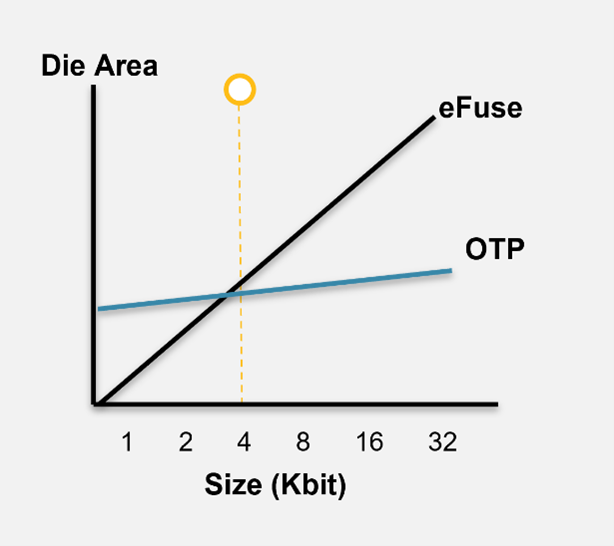
The earliest FuseBox was a set of metal fuses that were blown by high current to store the repair signature, also known as eFuses. But as technology evolves and as AI applications have become more sophisticated, requiring more SRAM capacity, the amount of SRAM that potentially needs repairing also increases. For AI applications implemented on 7nm (and below) process nodes, the prerequisite SRAM size ranges from the tens to hundreds of MB, which requires a repair capacity from the tens to hundreds of Kb, which determines the size of the FuseBox. At this point, anti-fuse based One-Time Programmable Memory (OTP) becomes the better choice to implement a FuseBox, especially for advanced processes. Why? Let's take eMemory's NeoFuse (Anti-fuse OTP) as an example, compared with eFuses.
For advanced process nodes, eMemory's NeoFuse OTP has the following advantages over eFuses:
- Small area: NeoFuse occupies a much smaller area than eFuse for applications that require several hundred Kb of capacity.
- Reliability: NeoFuse has no maximum number of reads limit while maintaining the highest reliability.
- Mass production yield: NeoFuse has the best yield and mass production record for large capacities.
- Simple integration: There is no requirement for users to add special high current circuitry, thus simplifying the layout and allowing for in-field OTP programming.
In conclusion, the larger the storage size requirements, the greater the advantages of NeoFuse, especially in terms of size and yield.

Figure 2: OTP versus eFuse: Density and Size
The Solution Simultaneously Considering Security Operations and Memory Repair for Advanced Applications
Even as the demand for SRAM repair increases dramatically with the development of advanced applications, the deployment of security cannot be ignored. eMemory and its subsidiary PUFsecurity, a leader in memory solutions and chip security, have incorporated FuseBox functionality into their hardware root-of-trust (RoT) solution, saving not only system area, but also reducing design cost and effort by offering security and SRAM repair in a single solution.
A RoT is a widely specified standard component for security architectures such as Arm's Confidential Computing Architecture, RISC-V's Keystone Trusted Execution Environment (TEE), and the PSA Certified Internet of Things Security Framework. In addition, the secure boot process described in the Unified Extensible Firmware Interface (UEFI) standard is anchored upon a Root of Trust.
Conclusions
In order to maintain high data throughputs, SoCs need fast, multi-core processors paired with high density SRAM caches. However, the high cost of SRAM failures has emphasized the importance of SRAM Repair capability as advanced manufacturing processes face increased yield and reliability challenges. At the same time, as advanced applications demand strong security, a solution that integrates these two requirements is undoubtedly a better choice for designers. So not only do eMemory and PUFsecurity’s solutions integrate a complete MBISR tool with their standard hardware root of trust, but every solution utilizes NeoFuse, a much superior memory when compared with eFuse, especially when it comes to yield and size. Thus, engineers’ design resources are saved, helping modern semiconductors meet the demand for secure computing and reliable memory in this booming era of AI.

